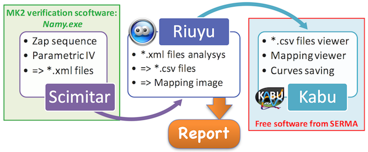
SERMA Activities
ESD Activities
Definitions:
- ESD : ElectroStatic Discharge
- HBM : (Human Body Model) An electrostatic discharge(ESD) event meeting the waveform criteria specified in standards, approximating the discharge from the fingertip of a typical human being to a grounded device
- MM : (Machine Model) An electrostatic discharge (ESD) used to simulate an event occurring from a low resistance source
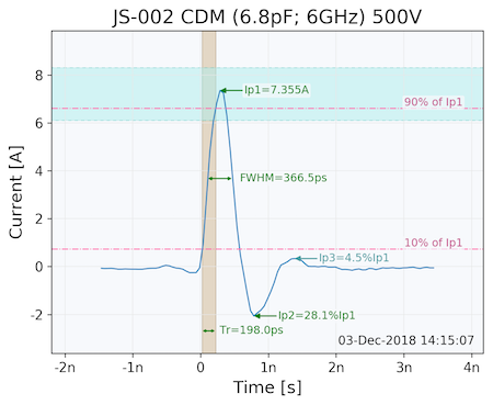
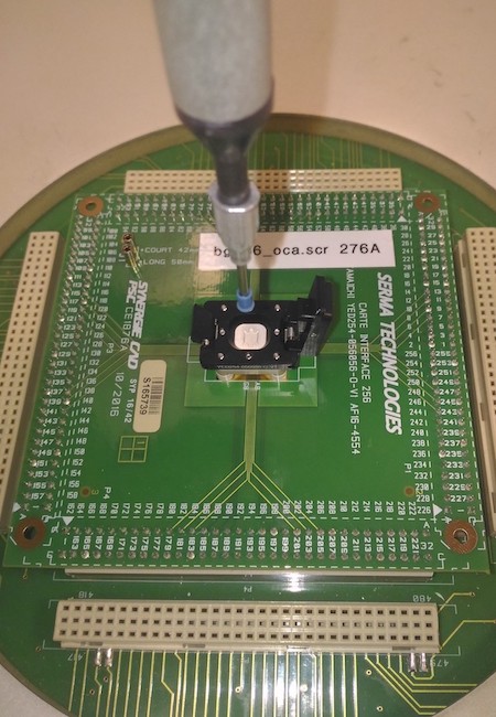
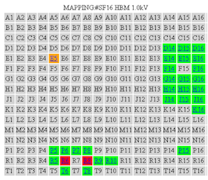
- CDM : (Charge Device Model) An electrostatic discharge (ESD) used to simulate the actual discharge event that occurs when a charged device is quickly discharged to another object at a lower electrostatic potential through a single pin or terminal
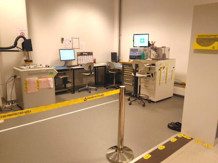
- EPA : ESD Protected Areas
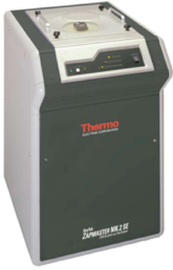
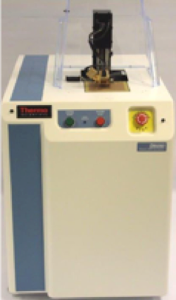
- ESD tester : Equipment that applies a HBM ESD (Thermo Keytek Zapmaster MK.2 SE) or a CDM ESD (Thermo Scientific Orion3) to a component
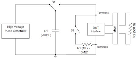
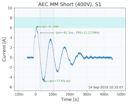
| Human Body Model (HBM) & Machine Model (MM) | ||
 |
SERMA Main Strength on HBM & MM tests
|
|
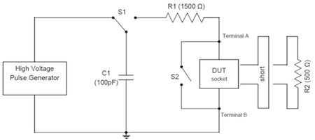 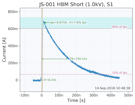 Human Body Model (HBM) Human Body Model (HBM) |
Systems Strengths ?
Model ?
|
|
 Machine Model (MM)
| Charged Device Model (CDM) | ||
 |
SERMA Main Strength on CDM tests
|
|
 |
Model ?
|
 |
| Additionnal information | ||
 |
|
 |
 |
 |
|

Serma Technologies : BHT - Bâtiment 52 - 7, Parvis Louis Néel – CS20050 - 38040 Grenoble – France
Customer Service: csc@serma.com ; +33 (0)5 57 26 08 88
LU Activities
Definitions:
- ESD : ElectroStatic Discharge
- LU : (Latch-Up) A state in which a low-impedance path, resulting from an overstress that triggers a parasitic thyristor structure, persists after removal or cessation of the triggering condition
- Vsupply overvoltage test: A latch-up test that supplies overvoltage pulses to the Vsupply pin (or pin group) under test
- Latch-up tester : Test equipment capable of performing the tests as specified in standards. For devices requiring dynamic testing, required timing signals and logic vectors may be applied by the latch-up tester itself, external equipment, and/or external components as appropriate
- Heat source : Equipment capable of heating and maintaining the DUT at the maximum operating temperature specified in the device specification during the latch-up test
- EPA : ESD Protected Areas
| Latch-up (LU) Tests | ||
|
SERMA Main Strength
|
|
|
Test Description
|
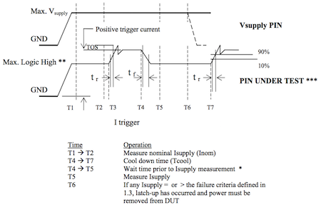 |
|
|
Systems Strengths ?
|
How ?
|
| Additionnal information | ||
|
|
|
![]()
Serma Technologies : BHT - Bâtiment 52 - 7, Parvis Louis Néel – CS20050 - 38040 Grenoble – France
Customer Service: csc@serma.com ; +33 (0)5 57 26 08 88
FIB Edit Activities
Definitions :
- FIB : Focused Ion Beam
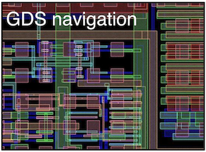
- GDS : (Graphic Database System) Files used in the FIB equipment to navigate to a specific area in the integreted circuit
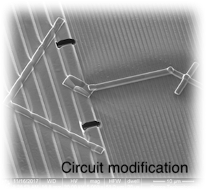
- Circuit Edit : Technique used in new design flow modifications on integreted circuit; This technique can be applied to design optimization changes before final productionin, debugging process or solutions fixes
 |
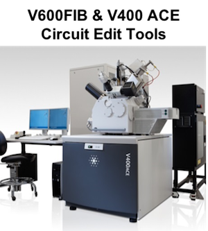
SERMA Main Strength
|
|
|
Systems Strengths ?
|
 |
Chemistries available ?
|
|
How ?
|
 |
Main uses ?
|
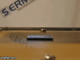
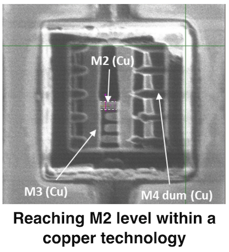
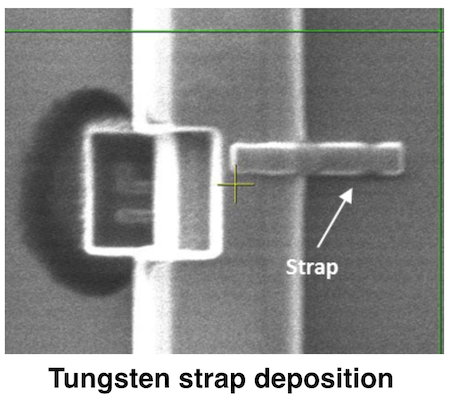
| Circuit-Edit examples | ||
|
|
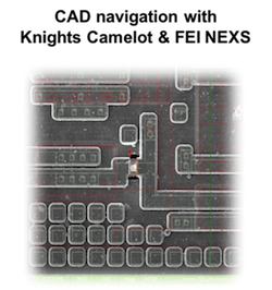
Using GDS files for navigation |
 |
![]() Serma Technologies : BHT - Bâtiment 52 - 7, Parvis Louis Néel – CS20050 - 38040 Grenoble – France
Serma Technologies : BHT - Bâtiment 52 - 7, Parvis Louis Néel – CS20050 - 38040 Grenoble – France
Customer Service: csc@serma.com ; +33 (0)5 57 26 08 88